A Scalable & Non-Destructive Characterization Strategy to Study Semiconductor/Dielectric Interfaces and Predict Wafer-Level Device Performance Article Swipe
 YOU?
·
· 2024
· Open Access
·
· DOI: https://doi.org/10.2172/2480157
YOU?
·
· 2024
· Open Access
·
· DOI: https://doi.org/10.2172/2480157
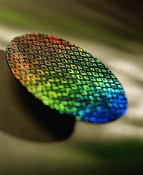
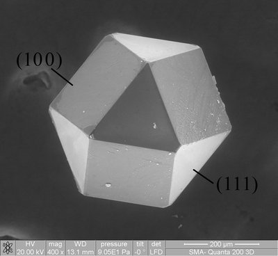
The defect density present at the dielectric-semiconductor interface in an MOS structure directly influences the channel carrier characteristics in semiconductor devices, especially in wide bandgap material systems used in power devices. While these trap defects are typically quantified through electrical characterization of MOS-capacitor test structures, this treatment offers very little insight into the physical nature of interface defects. Such shortcomings demand a physical characterization strategy to guide fabrication optimization. X-ray photoelectron spectroscopy (XPS) is suggested as a viable technique to determine chemical data for dielectric interfaces formed using atomic layer deposition (ALD) on GaN substrates. Previously, 1-D XPS characterization has confirmed the presence of a GaxOy interlayer between ALD dielectrics and the GaN substrate. In this work, XPS data is serially collected to form 2-D images of an ALD-Al2O3/GaN interface as a proof-of-concept experiment for in-situ XPS quality monitoring during ALD processing. The information provided by this work reveals some of the challenges for incorporating XPS characterization as an in-situ strategy during fabrication of GaN-based devices. Separately, electrical mapping of a 2-D array of ALD-Al2O3/GaN MOS-capacitor devices provide a means to quantify the spatial variations in interface quality across a single wafer. Physical characterization techniques, such as time-of-flight secondary ion mass spectroscopy, provide additional chemical information about the Al2O3/GaxOy/GaN structure that complement the electrical mapping results. This analysis shows that a higher GaxOy content correlates with higher interface state defects for trap energies deep in the band gap.
Related Topics

- Type
- report
- Language
- en
- Landing Page
- https://doi.org/10.2172/2480157
- OA Status
- green
- Related Works
- 10
- OpenAlex ID
- https://openalex.org/W4405296141
Raw OpenAlex JSON
- OpenAlex ID
-
https://openalex.org/W4405296141Canonical identifier for this work in OpenAlex
- DOI
-
https://doi.org/10.2172/2480157Digital Object Identifier
- Title
-
A Scalable & Non-Destructive Characterization Strategy to Study Semiconductor/Dielectric Interfaces and Predict Wafer-Level Device PerformanceWork title
- Type
-
reportOpenAlex work type
- Language
-
enPrimary language
- Publication year
-
2024Year of publication
- Publication date
-
2024-11-01Full publication date if available
- Authors
-
Brian Rummel, Melissa Meyerson, Caleb Glaser, Joseph P. KleskoList of authors in order
- Landing page
-
https://doi.org/10.2172/2480157Publisher landing page
- Open access
-
YesWhether a free full text is available
- OA status
-
greenOpen access status per OpenAlex
- OA URL
-
https://www.osti.gov/biblio/2480157Direct OA link when available
- Concepts
-
Wafer, Characterization (materials science), Dielectric, Materials science, Semiconductor, Scalability, Optoelectronics, Electronic engineering, Computer science, Nanotechnology, Engineering, DatabaseTop concepts (fields/topics) attached by OpenAlex
- Cited by
-
0Total citation count in OpenAlex
- Related works (count)
-
10Other works algorithmically related by OpenAlex
Full payload
| id | https://openalex.org/W4405296141 |
|---|---|
| doi | https://doi.org/10.2172/2480157 |
| ids.doi | https://doi.org/10.2172/2480157 |
| ids.openalex | https://openalex.org/W4405296141 |
| fwci | |
| type | report |
| title | A Scalable & Non-Destructive Characterization Strategy to Study Semiconductor/Dielectric Interfaces and Predict Wafer-Level Device Performance |
| biblio.issue | |
| biblio.volume | |
| biblio.last_page | |
| biblio.first_page | |
| topics[0].id | https://openalex.org/T10623 |
| topics[0].field.id | https://openalex.org/fields/22 |
| topics[0].field.display_name | Engineering |
| topics[0].score | 0.989300012588501 |
| topics[0].domain.id | https://openalex.org/domains/3 |
| topics[0].domain.display_name | Physical Sciences |
| topics[0].subfield.id | https://openalex.org/subfields/2208 |
| topics[0].subfield.display_name | Electrical and Electronic Engineering |
| topics[0].display_name | Thin-Film Transistor Technologies |
| topics[1].id | https://openalex.org/T11527 |
| topics[1].field.id | https://openalex.org/fields/22 |
| topics[1].field.display_name | Engineering |
| topics[1].score | 0.9836999773979187 |
| topics[1].domain.id | https://openalex.org/domains/3 |
| topics[1].domain.display_name | Physical Sciences |
| topics[1].subfield.id | https://openalex.org/subfields/2208 |
| topics[1].subfield.display_name | Electrical and Electronic Engineering |
| topics[1].display_name | 3D IC and TSV technologies |
| topics[2].id | https://openalex.org/T11853 |
| topics[2].field.id | https://openalex.org/fields/31 |
| topics[2].field.display_name | Physics and Astronomy |
| topics[2].score | 0.9825999736785889 |
| topics[2].domain.id | https://openalex.org/domains/3 |
| topics[2].domain.display_name | Physical Sciences |
| topics[2].subfield.id | https://openalex.org/subfields/3107 |
| topics[2].subfield.display_name | Atomic and Molecular Physics, and Optics |
| topics[2].display_name | Semiconductor materials and interfaces |
| is_xpac | False |
| apc_list | |
| apc_paid | |
| concepts[0].id | https://openalex.org/C160671074 |
| concepts[0].level | 2 |
| concepts[0].score | 0.7645391821861267 |
| concepts[0].wikidata | https://www.wikidata.org/wiki/Q267131 |
| concepts[0].display_name | Wafer |
| concepts[1].id | https://openalex.org/C2780841128 |
| concepts[1].level | 2 |
| concepts[1].score | 0.6779605746269226 |
| concepts[1].wikidata | https://www.wikidata.org/wiki/Q5073781 |
| concepts[1].display_name | Characterization (materials science) |
| concepts[2].id | https://openalex.org/C133386390 |
| concepts[2].level | 2 |
| concepts[2].score | 0.6460686326026917 |
| concepts[2].wikidata | https://www.wikidata.org/wiki/Q184996 |
| concepts[2].display_name | Dielectric |
| concepts[3].id | https://openalex.org/C192562407 |
| concepts[3].level | 0 |
| concepts[3].score | 0.6216694116592407 |
| concepts[3].wikidata | https://www.wikidata.org/wiki/Q228736 |
| concepts[3].display_name | Materials science |
| concepts[4].id | https://openalex.org/C108225325 |
| concepts[4].level | 2 |
| concepts[4].score | 0.6126600503921509 |
| concepts[4].wikidata | https://www.wikidata.org/wiki/Q11456 |
| concepts[4].display_name | Semiconductor |
| concepts[5].id | https://openalex.org/C48044578 |
| concepts[5].level | 2 |
| concepts[5].score | 0.5974865555763245 |
| concepts[5].wikidata | https://www.wikidata.org/wiki/Q727490 |
| concepts[5].display_name | Scalability |
| concepts[6].id | https://openalex.org/C49040817 |
| concepts[6].level | 1 |
| concepts[6].score | 0.5552534461021423 |
| concepts[6].wikidata | https://www.wikidata.org/wiki/Q193091 |
| concepts[6].display_name | Optoelectronics |
| concepts[7].id | https://openalex.org/C24326235 |
| concepts[7].level | 1 |
| concepts[7].score | 0.43279507756233215 |
| concepts[7].wikidata | https://www.wikidata.org/wiki/Q126095 |
| concepts[7].display_name | Electronic engineering |
| concepts[8].id | https://openalex.org/C41008148 |
| concepts[8].level | 0 |
| concepts[8].score | 0.36164915561676025 |
| concepts[8].wikidata | https://www.wikidata.org/wiki/Q21198 |
| concepts[8].display_name | Computer science |
| concepts[9].id | https://openalex.org/C171250308 |
| concepts[9].level | 1 |
| concepts[9].score | 0.330931156873703 |
| concepts[9].wikidata | https://www.wikidata.org/wiki/Q11468 |
| concepts[9].display_name | Nanotechnology |
| concepts[10].id | https://openalex.org/C127413603 |
| concepts[10].level | 0 |
| concepts[10].score | 0.19851094484329224 |
| concepts[10].wikidata | https://www.wikidata.org/wiki/Q11023 |
| concepts[10].display_name | Engineering |
| concepts[11].id | https://openalex.org/C77088390 |
| concepts[11].level | 1 |
| concepts[11].score | 0.05004227161407471 |
| concepts[11].wikidata | https://www.wikidata.org/wiki/Q8513 |
| concepts[11].display_name | Database |
| keywords[0].id | https://openalex.org/keywords/wafer |
| keywords[0].score | 0.7645391821861267 |
| keywords[0].display_name | Wafer |
| keywords[1].id | https://openalex.org/keywords/characterization |
| keywords[1].score | 0.6779605746269226 |
| keywords[1].display_name | Characterization (materials science) |
| keywords[2].id | https://openalex.org/keywords/dielectric |
| keywords[2].score | 0.6460686326026917 |
| keywords[2].display_name | Dielectric |
| keywords[3].id | https://openalex.org/keywords/materials-science |
| keywords[3].score | 0.6216694116592407 |
| keywords[3].display_name | Materials science |
| keywords[4].id | https://openalex.org/keywords/semiconductor |
| keywords[4].score | 0.6126600503921509 |
| keywords[4].display_name | Semiconductor |
| keywords[5].id | https://openalex.org/keywords/scalability |
| keywords[5].score | 0.5974865555763245 |
| keywords[5].display_name | Scalability |
| keywords[6].id | https://openalex.org/keywords/optoelectronics |
| keywords[6].score | 0.5552534461021423 |
| keywords[6].display_name | Optoelectronics |
| keywords[7].id | https://openalex.org/keywords/electronic-engineering |
| keywords[7].score | 0.43279507756233215 |
| keywords[7].display_name | Electronic engineering |
| keywords[8].id | https://openalex.org/keywords/computer-science |
| keywords[8].score | 0.36164915561676025 |
| keywords[8].display_name | Computer science |
| keywords[9].id | https://openalex.org/keywords/nanotechnology |
| keywords[9].score | 0.330931156873703 |
| keywords[9].display_name | Nanotechnology |
| keywords[10].id | https://openalex.org/keywords/engineering |
| keywords[10].score | 0.19851094484329224 |
| keywords[10].display_name | Engineering |
| keywords[11].id | https://openalex.org/keywords/database |
| keywords[11].score | 0.05004227161407471 |
| keywords[11].display_name | Database |
| language | en |
| locations[0].id | doi:10.2172/2480157 |
| locations[0].is_oa | False |
| locations[0].source | |
| locations[0].license | |
| locations[0].pdf_url | |
| locations[0].version | publishedVersion |
| locations[0].raw_type | report |
| locations[0].license_id | |
| locations[0].is_accepted | True |
| locations[0].is_published | True |
| locations[0].raw_source_name | |
| locations[0].landing_page_url | https://doi.org/10.2172/2480157 |
| locations[1].id | pmh:oai:osti.gov:2480157 |
| locations[1].is_oa | True |
| locations[1].source.id | https://openalex.org/S4306402487 |
| locations[1].source.issn | |
| locations[1].source.type | repository |
| locations[1].source.is_oa | False |
| locations[1].source.issn_l | |
| locations[1].source.is_core | False |
| locations[1].source.is_in_doaj | False |
| locations[1].source.display_name | OSTI OAI (U.S. Department of Energy Office of Scientific and Technical Information) |
| locations[1].source.host_organization | https://openalex.org/I139351228 |
| locations[1].source.host_organization_name | Office of Scientific and Technical Information |
| locations[1].source.host_organization_lineage | https://openalex.org/I139351228 |
| locations[1].license | |
| locations[1].pdf_url | https://www.osti.gov/biblio/2480157 |
| locations[1].version | submittedVersion |
| locations[1].raw_type | |
| locations[1].license_id | |
| locations[1].is_accepted | False |
| locations[1].is_published | False |
| locations[1].raw_source_name | |
| locations[1].landing_page_url | https://www.osti.gov/biblio/2480157 |
| indexed_in | crossref |
| authorships[0].author.id | https://openalex.org/A5087296420 |
| authorships[0].author.orcid | https://orcid.org/0000-0002-0161-5774 |
| authorships[0].author.display_name | Brian Rummel |
| authorships[0].countries | US |
| authorships[0].affiliations[0].institution_ids | https://openalex.org/I4210104735 |
| authorships[0].affiliations[0].raw_affiliation_string | Sandia National Laboratories (SNL-NM), Albuquerque, NM (United States) |
| authorships[0].institutions[0].id | https://openalex.org/I4210104735 |
| authorships[0].institutions[0].ror | https://ror.org/01apwpt12 |
| authorships[0].institutions[0].type | facility |
| authorships[0].institutions[0].lineage | https://openalex.org/I1330989302, https://openalex.org/I198811213, https://openalex.org/I4210104735 |
| authorships[0].institutions[0].country_code | US |
| authorships[0].institutions[0].display_name | Sandia National Laboratories |
| authorships[0].author_position | first |
| authorships[0].raw_author_name | Brian Rummel |
| authorships[0].is_corresponding | False |
| authorships[0].raw_affiliation_strings | Sandia National Laboratories (SNL-NM), Albuquerque, NM (United States) |
| authorships[1].author.id | https://openalex.org/A5080170507 |
| authorships[1].author.orcid | https://orcid.org/0000-0001-9327-442X |
| authorships[1].author.display_name | Melissa Meyerson |
| authorships[1].countries | US |
| authorships[1].affiliations[0].institution_ids | https://openalex.org/I4210104735 |
| authorships[1].affiliations[0].raw_affiliation_string | Sandia National Laboratories (SNL-NM), Albuquerque, NM (United States) |
| authorships[1].institutions[0].id | https://openalex.org/I4210104735 |
| authorships[1].institutions[0].ror | https://ror.org/01apwpt12 |
| authorships[1].institutions[0].type | facility |
| authorships[1].institutions[0].lineage | https://openalex.org/I1330989302, https://openalex.org/I198811213, https://openalex.org/I4210104735 |
| authorships[1].institutions[0].country_code | US |
| authorships[1].institutions[0].display_name | Sandia National Laboratories |
| authorships[1].author_position | middle |
| authorships[1].raw_author_name | Melissa Meyerson |
| authorships[1].is_corresponding | False |
| authorships[1].raw_affiliation_strings | Sandia National Laboratories (SNL-NM), Albuquerque, NM (United States) |
| authorships[2].author.id | https://openalex.org/A5048676927 |
| authorships[2].author.orcid | https://orcid.org/0009-0004-9663-2674 |
| authorships[2].author.display_name | Caleb Glaser |
| authorships[2].countries | US |
| authorships[2].affiliations[0].institution_ids | https://openalex.org/I4210104735 |
| authorships[2].affiliations[0].raw_affiliation_string | Sandia National Laboratories (SNL-NM), Albuquerque, NM (United States) |
| authorships[2].institutions[0].id | https://openalex.org/I4210104735 |
| authorships[2].institutions[0].ror | https://ror.org/01apwpt12 |
| authorships[2].institutions[0].type | facility |
| authorships[2].institutions[0].lineage | https://openalex.org/I1330989302, https://openalex.org/I198811213, https://openalex.org/I4210104735 |
| authorships[2].institutions[0].country_code | US |
| authorships[2].institutions[0].display_name | Sandia National Laboratories |
| authorships[2].author_position | middle |
| authorships[2].raw_author_name | Caleb Glaser |
| authorships[2].is_corresponding | False |
| authorships[2].raw_affiliation_strings | Sandia National Laboratories (SNL-NM), Albuquerque, NM (United States) |
| authorships[3].author.id | https://openalex.org/A5008199290 |
| authorships[3].author.orcid | https://orcid.org/0000-0003-3989-8009 |
| authorships[3].author.display_name | Joseph P. Klesko |
| authorships[3].countries | US |
| authorships[3].affiliations[0].institution_ids | https://openalex.org/I4210104735 |
| authorships[3].affiliations[0].raw_affiliation_string | Sandia National Laboratories (SNL-NM), Albuquerque, NM (United States) |
| authorships[3].institutions[0].id | https://openalex.org/I4210104735 |
| authorships[3].institutions[0].ror | https://ror.org/01apwpt12 |
| authorships[3].institutions[0].type | facility |
| authorships[3].institutions[0].lineage | https://openalex.org/I1330989302, https://openalex.org/I198811213, https://openalex.org/I4210104735 |
| authorships[3].institutions[0].country_code | US |
| authorships[3].institutions[0].display_name | Sandia National Laboratories |
| authorships[3].author_position | last |
| authorships[3].raw_author_name | Joseph Klesko |
| authorships[3].is_corresponding | False |
| authorships[3].raw_affiliation_strings | Sandia National Laboratories (SNL-NM), Albuquerque, NM (United States) |
| has_content.pdf | True |
| has_content.grobid_xml | True |
| is_paratext | False |
| open_access.is_oa | True |
| open_access.oa_url | https://www.osti.gov/biblio/2480157 |
| open_access.oa_status | green |
| open_access.any_repository_has_fulltext | False |
| created_date | 2025-10-10T00:00:00 |
| display_name | A Scalable & Non-Destructive Characterization Strategy to Study Semiconductor/Dielectric Interfaces and Predict Wafer-Level Device Performance |
| has_fulltext | True |
| is_retracted | False |
| updated_date | 2025-11-06T03:46:38.306776 |
| primary_topic.id | https://openalex.org/T10623 |
| primary_topic.field.id | https://openalex.org/fields/22 |
| primary_topic.field.display_name | Engineering |
| primary_topic.score | 0.989300012588501 |
| primary_topic.domain.id | https://openalex.org/domains/3 |
| primary_topic.domain.display_name | Physical Sciences |
| primary_topic.subfield.id | https://openalex.org/subfields/2208 |
| primary_topic.subfield.display_name | Electrical and Electronic Engineering |
| primary_topic.display_name | Thin-Film Transistor Technologies |
| related_works | https://openalex.org/W3107994849, https://openalex.org/W1998662473, https://openalex.org/W1988252515, https://openalex.org/W4247143848, https://openalex.org/W2075391483, https://openalex.org/W2009883749, https://openalex.org/W2735573198, https://openalex.org/W2742348144, https://openalex.org/W29442446, https://openalex.org/W2038820605 |
| cited_by_count | 0 |
| locations_count | 2 |
| best_oa_location.id | pmh:oai:osti.gov:2480157 |
| best_oa_location.is_oa | True |
| best_oa_location.source.id | https://openalex.org/S4306402487 |
| best_oa_location.source.issn | |
| best_oa_location.source.type | repository |
| best_oa_location.source.is_oa | False |
| best_oa_location.source.issn_l | |
| best_oa_location.source.is_core | False |
| best_oa_location.source.is_in_doaj | False |
| best_oa_location.source.display_name | OSTI OAI (U.S. Department of Energy Office of Scientific and Technical Information) |
| best_oa_location.source.host_organization | https://openalex.org/I139351228 |
| best_oa_location.source.host_organization_name | Office of Scientific and Technical Information |
| best_oa_location.source.host_organization_lineage | https://openalex.org/I139351228 |
| best_oa_location.license | |
| best_oa_location.pdf_url | https://www.osti.gov/biblio/2480157 |
| best_oa_location.version | submittedVersion |
| best_oa_location.raw_type | |
| best_oa_location.license_id | |
| best_oa_location.is_accepted | False |
| best_oa_location.is_published | False |
| best_oa_location.raw_source_name | |
| best_oa_location.landing_page_url | https://www.osti.gov/biblio/2480157 |
| primary_location.id | doi:10.2172/2480157 |
| primary_location.is_oa | False |
| primary_location.source | |
| primary_location.license | |
| primary_location.pdf_url | |
| primary_location.version | publishedVersion |
| primary_location.raw_type | report |
| primary_location.license_id | |
| primary_location.is_accepted | True |
| primary_location.is_published | True |
| primary_location.raw_source_name | |
| primary_location.landing_page_url | https://doi.org/10.2172/2480157 |
| publication_date | 2024-11-01 |
| publication_year | 2024 |
| referenced_works_count | 0 |
| abstract_inverted_index.a | 61, 76, 104, 131, 170, 178, 189, 220 |
| abstract_inverted_index.In | 114 |
| abstract_inverted_index.an | 9, 127, 158 |
| abstract_inverted_index.as | 75, 130, 157, 196 |
| abstract_inverted_index.at | 4 |
| abstract_inverted_index.by | 145 |
| abstract_inverted_index.in | 8, 18, 22, 28, 185, 234 |
| abstract_inverted_index.is | 73, 119 |
| abstract_inverted_index.of | 41, 55, 103, 126, 150, 163, 169, 173 |
| abstract_inverted_index.on | 92 |
| abstract_inverted_index.to | 65, 79, 122, 180 |
| abstract_inverted_index.1-D | 96 |
| abstract_inverted_index.2-D | 124, 171 |
| abstract_inverted_index.ALD | 108, 140 |
| abstract_inverted_index.GaN | 93, 112 |
| abstract_inverted_index.MOS | 10 |
| abstract_inverted_index.The | 0, 142 |
| abstract_inverted_index.XPS | 97, 117, 136, 155 |
| abstract_inverted_index.and | 110 |
| abstract_inverted_index.are | 35 |
| abstract_inverted_index.for | 83, 134, 153, 230 |
| abstract_inverted_index.has | 99 |
| abstract_inverted_index.ion | 199 |
| abstract_inverted_index.the | 5, 14, 52, 101, 111, 151, 182, 207, 212, 235 |
| abstract_inverted_index.Such | 58 |
| abstract_inverted_index.This | 216 |
| abstract_inverted_index.band | 236 |
| abstract_inverted_index.data | 82, 118 |
| abstract_inverted_index.deep | 233 |
| abstract_inverted_index.form | 123 |
| abstract_inverted_index.gap. | 237 |
| abstract_inverted_index.into | 51 |
| abstract_inverted_index.mass | 200 |
| abstract_inverted_index.some | 149 |
| abstract_inverted_index.such | 195 |
| abstract_inverted_index.test | 43 |
| abstract_inverted_index.that | 210, 219 |
| abstract_inverted_index.this | 45, 115, 146 |
| abstract_inverted_index.trap | 33, 231 |
| abstract_inverted_index.used | 27 |
| abstract_inverted_index.very | 48 |
| abstract_inverted_index.wide | 23 |
| abstract_inverted_index.with | 225 |
| abstract_inverted_index.work | 147 |
| abstract_inverted_index.(ALD) | 91 |
| abstract_inverted_index.(XPS) | 72 |
| abstract_inverted_index.While | 31 |
| abstract_inverted_index.X-ray | 69 |
| abstract_inverted_index.about | 206 |
| abstract_inverted_index.array | 172 |
| abstract_inverted_index.guide | 66 |
| abstract_inverted_index.layer | 89 |
| abstract_inverted_index.means | 179 |
| abstract_inverted_index.power | 29 |
| abstract_inverted_index.shows | 218 |
| abstract_inverted_index.state | 228 |
| abstract_inverted_index.these | 32 |
| abstract_inverted_index.using | 87 |
| abstract_inverted_index.work, | 116 |
| abstract_inverted_index.across | 188 |
| abstract_inverted_index.atomic | 88 |
| abstract_inverted_index.defect | 1 |
| abstract_inverted_index.demand | 60 |
| abstract_inverted_index.during | 139, 161 |
| abstract_inverted_index.formed | 86 |
| abstract_inverted_index.higher | 221, 226 |
| abstract_inverted_index.images | 125 |
| abstract_inverted_index.little | 49 |
| abstract_inverted_index.nature | 54 |
| abstract_inverted_index.offers | 47 |
| abstract_inverted_index.single | 190 |
| abstract_inverted_index.viable | 77 |
| abstract_inverted_index.wafer. | 191 |
| abstract_inverted_index.bandgap | 24 |
| abstract_inverted_index.between | 107 |
| abstract_inverted_index.carrier | 16 |
| abstract_inverted_index.channel | 15 |
| abstract_inverted_index.content | 223 |
| abstract_inverted_index.defects | 34, 229 |
| abstract_inverted_index.density | 2 |
| abstract_inverted_index.devices | 176 |
| abstract_inverted_index.in-situ | 135, 159 |
| abstract_inverted_index.insight | 50 |
| abstract_inverted_index.mapping | 168, 214 |
| abstract_inverted_index.present | 3 |
| abstract_inverted_index.provide | 177, 202 |
| abstract_inverted_index.quality | 137, 187 |
| abstract_inverted_index.reveals | 148 |
| abstract_inverted_index.spatial | 183 |
| abstract_inverted_index.systems | 26 |
| abstract_inverted_index.through | 38 |
| abstract_inverted_index.Physical | 192 |
| abstract_inverted_index.analysis | 217 |
| abstract_inverted_index.chemical | 81, 204 |
| abstract_inverted_index.defects. | 57 |
| abstract_inverted_index.devices, | 20 |
| abstract_inverted_index.devices. | 30, 165 |
| abstract_inverted_index.directly | 12 |
| abstract_inverted_index.energies | 232 |
| abstract_inverted_index.material | 25 |
| abstract_inverted_index.physical | 53, 62 |
| abstract_inverted_index.presence | 102 |
| abstract_inverted_index.provided | 144 |
| abstract_inverted_index.quantify | 181 |
| abstract_inverted_index.results. | 215 |
| abstract_inverted_index.serially | 120 |
| abstract_inverted_index.strategy | 64, 160 |
| abstract_inverted_index.GaN-based | 164 |
| abstract_inverted_index.collected | 121 |
| abstract_inverted_index.confirmed | 100 |
| abstract_inverted_index.determine | 80 |
| abstract_inverted_index.interface | 7, 56, 129, 186, 227 |
| abstract_inverted_index.secondary | 198 |
| abstract_inverted_index.structure | 11, 209 |
| abstract_inverted_index.suggested | 74 |
| abstract_inverted_index.technique | 78 |
| abstract_inverted_index.treatment | 46 |
| abstract_inverted_index.typically | 36 |
| abstract_inverted_index.additional | 203 |
| abstract_inverted_index.challenges | 152 |
| abstract_inverted_index.complement | 211 |
| abstract_inverted_index.correlates | 224 |
| abstract_inverted_index.deposition | 90 |
| abstract_inverted_index.dielectric | 84 |
| abstract_inverted_index.electrical | 39, 167, 213 |
| abstract_inverted_index.especially | 21 |
| abstract_inverted_index.experiment | 133 |
| abstract_inverted_index.influences | 13 |
| abstract_inverted_index.interfaces | 85 |
| abstract_inverted_index.interlayer | 106 |
| abstract_inverted_index.monitoring | 138 |
| abstract_inverted_index.quantified | 37 |
| abstract_inverted_index.substrate. | 113 |
| abstract_inverted_index.variations | 184 |
| abstract_inverted_index.Previously, | 95 |
| abstract_inverted_index.Separately, | 166 |
| abstract_inverted_index.dielectrics | 109 |
| abstract_inverted_index.fabrication | 67, 162 |
| abstract_inverted_index.information | 143, 205 |
| abstract_inverted_index.processing. | 141 |
| abstract_inverted_index.structures, | 44 |
| abstract_inverted_index.substrates. | 94 |
| abstract_inverted_index.techniques, | 194 |
| abstract_inverted_index.shortcomings | 59 |
| abstract_inverted_index.spectroscopy | 71 |
| abstract_inverted_index.MOS-capacitor | 42, 175 |
| abstract_inverted_index.incorporating | 154 |
| abstract_inverted_index.optimization. | 68 |
| abstract_inverted_index.photoelectron | 70 |
| abstract_inverted_index.semiconductor | 19 |
| abstract_inverted_index.spectroscopy, | 201 |
| abstract_inverted_index.time-of-flight | 197 |
| abstract_inverted_index.characteristics | 17 |
| abstract_inverted_index.characterization | 40, 63, 98, 156, 193 |
| abstract_inverted_index.proof-of-concept | 132 |
| abstract_inverted_index.dielectric-semiconductor | 6 |
| abstract_inverted_index.Ga<sub>x</sub>O<sub>y</sub> | 105, 222 |
| abstract_inverted_index.ALD-Al<sub>2</sub>O<sub>3</sub>/GaN | 128, 174 |
| abstract_inverted_index.Al<sub>2</sub>O<sub>3</sub>/Ga<sub>x</sub>O<sub>y</sub>/GaN | 208 |
| cited_by_percentile_year | |
| countries_distinct_count | 1 |
| institutions_distinct_count | 4 |
| citation_normalized_percentile |